0

|
|
The AD5379 offers guaranteed operation over a wide V(SS)/V(DD) supply range from ±11.4 V to ±16.5 V. The output amplifier headroom requirement is 2.5 V operating with a load current of 1.5 mA, and 2 V operating with a load current of 0.5 mA.
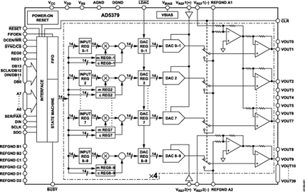
The AD5379 contains a double-buffered parallel interface in which 14 data bits are loaded into one of the input registers under the control of theWR,CS, and DAC Channel Address Pins A0 to A7. It also has a 3-wire serial interface that is com-patible with SPI , QSPI , MICROWIRE , and DSP interface standards and can handle clock speeds of up to 50 MHz.
The DAC outputs are updated upon reception of new data into the DAC registers. All the outputs can be simultaneously updated by taking theLDACinput low. Each channel has a programmable gain and an offset adjust register.
Each DAC output is gained and buffered on-chip with respect to an external REFGND input. The DAC outputs can also be switched to REFGND via theCLRpin.
Applications
【用 途】 【性能 参数】【互换 兼容】
Analog Devices公司的AD5379是一种具有40个通道的14位DAC(数/模变换器),装入13×13mm封装中,适用于需要很多输出通道的ATE(自动测试设备)、光联网络设备和控制设备。AD5379包括为每个通道提供增益的输出放大器。它是单片集成电路,精度达到12位。该DAC的输出范围可通过选择正负两个基准电压来确定。最大输出电压范围为17.5V。