0

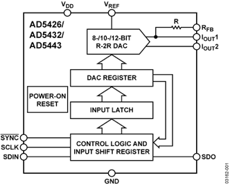
The AD5426/AD5432/AD5443 are CMOS 8-, 10-, and 12-bit current output digital-to- converters (DACs), respectively. These devices operate from a 2.5 V to 5.5 V power supply, making them suitable for battery-powered applications and many other applications.
These DACs use a double buffered, 3-wire serial interface that is compatible with SPI, QSPI , MICROWIRE , and most DSP interface standards. In addition, a serial data out pin (SDO) allows for daisy-chaining when multiple packages are used. Data readback allows the user to read the contents of the DAC register via the SDO pin. On power-up, the internal shift register and latches are filled with 0s and the DAC outputs are at zero scale.
As a result of manufacturing on a CMOS submicron process, the parts offer excellent 4-quadrant multiplication characteristics with large signal multiplying bandwidths of 10 MHz. The applied external reference input voltage, VREF, determines the full-scale output current. An integrated feedback resistor, RFB, provides temperature tracking and full-scale voltage output when combined with an external current to voltage precision amplifier.
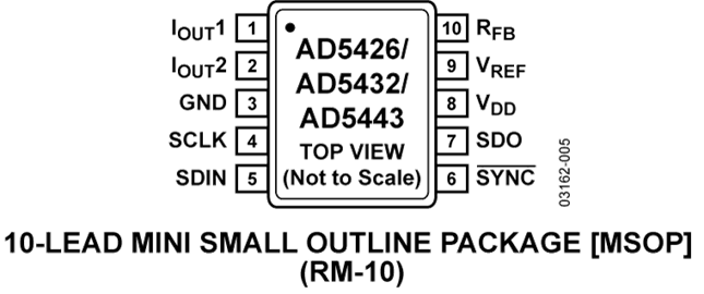
The AD5426/AD5432/AD5443 DACs are available in small, 10-lead MSOP packages.
The EVAL-AD5443SDZ/EVAL-AD5446SDZ/EVAL-AD5453SDZ evaluation board is available for evaluating DAC performance. For more information, see the UG-327 evaluation board user guide.
Applications
【用 途】 【性能 参数】【互换 兼容】
本文所述 电路 为一种高性能、单极性、精密直流DAC配置,采用 AD5426 / AD5432 / AD5443 系列精密乘法DAC、低噪声 运算放大器 AD8065 以及精密基准电压源
电路 功能与优势 本电路采用精密乘法DAC和低噪声 运算放大器 ,构成双极性、精密直流DAC配置。DAC是核心可编程元件,所选的 放大器 可决定精度或速度性能。对于精密、高精度、低噪声应用,可以用 AD8066 等双通道运算放大器来提供电流电压转换和双极性输出。图1:双极性精密直流转换(原理示意图) 电路描述
电路 功能与优势 本电路利用乘法DAC和 运算放大器 提供可编程增益功能。最大增益值和温度系数由外部 电阻 设置,可编程增益的分辨率由DAC的分辨率设置。图1:采用电流输出DAC的可编程增益电路(原理示意图) 电路描述 图1所示电路就是推荐用来提高电路增益的方法。R1、R2和R3应具有相似的温度系数,但不必与DAC的温