华强商城 被动器件(电容/电阻/电感) BOM配单 原厂专区 PCB制板 积分兑换
0
首页>IC索引

AD9257S

Octal, 14-Bit, 65 MSPS Serial LVDS 1.8 V -to-Digital Converter

AD9257S产品信息:

概览

优势和特点

  • Low power: 55 mW per channel at 65 MSPS with scalable power options
  • SNR = 75.5 dB (to Nyquist)
  • SFDR = 91 dBc (to Nyquist)
  • DNL = ±0.6 LSB (typical), INL = ±1.1 LSB (typical)
  • Serial LVDS (ANSI-644, default)
    • Low power, reduced signal option (similar to IEEE 1596.3)
  • Data and frame clock outputs
  • 650 MHz full power bandwidth
  • 2 V p-p input voltage range
  • 1.8 V supply operation
  • Serial port control
    • Full chip and individual channel power-down modes
    • Flexible bit orientation
    • Built-in and custom digital test pattern generation
    • Programmable clock and data alignment
    • Programmable output resolution
    • Standby mode

Commercial Space Features

  • Military temperature range (-55°C to +125°C)
  • Wafer diffusion lot traceability
  • Radiation lot acceptance test (RLAT)
    • Total ionizing dose (TID)
  • Radiation benchmark
    • Single event latch-up (SEL)

产品详情

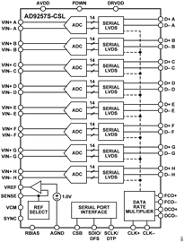
The AD9257S-CSL is an octal, 14-bit, 65 MSPS -to-digital converter (ADC) with an on-chip sample-and-hold circuit designed for low cost, low power, small size, and ease of use. The product operates at a conversion rate of up to 65 MSPS and is optimized for outstanding dynamic performance and low power in applications where a small package size is critical.

The ADC requires a single 1.8 V power supply and low voltage, positive emitter-coupled logic (LVPECL)-/ CMOS-/low voltage differential signaling (LVDS)-compatible sample rate clock for full performance operation. No external reference or driver components are required for many applications.

The ADC automatically multiplies the sample rate clock for the appropriate LVDS serial data rate. A data clock output (DCO) for capturing data on the output and a frame clock output (FCO) for signaling a new output byte are provided. Individual channel power-down is supported and typically consumes 1 mW when all channels are disabled. The ADC contains several features designed to maximize flexibility and minimize system cost, such as programmable clock and data alignment and programmable digital test pattern generation. The available digital test patterns include built-in deterministic and pseudorandom patterns, along with custom user-defined test patterns entered via the serial port interface (SPI).

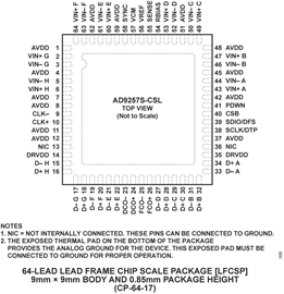
The AD9257S-CSL is available in an RoHS-compliant, 64-lead lead frame chip scale package (LFCSP). The device is specified over the -55°C to +125°C temperature range. This product is protected by a U.S. patent. Additional application and technical information can be found in the Commercial Space Products Program brochure and the AD9257 data sheet.

PRODUCT HIGHLIGHTS

  1. Small Footprint. Eight ADCs are contained in a small, space-saving package.
  2. Low Power of 55 mW/Channel at 65 MSPS with Scalable Power Options.
  3. Ease of Use. A DCO is provided that operates at frequencies of up to 455 MHz and supports double data rate (DDR) operation.
  4. User Flexibility. The SPI control offers a wide range of flexible features to meet specific system requirements.
  5. Pin Compatible with the AD9637 (12-Bit Octal ADC).

APPLICATIONS

  • Low Earth orbit (LEO) space payloads
  • Quadrature and diversity radio receiver
  • Optical imaging

AD9257S数据手册:

AD9257S引脚功能、电路图:

相关型号:

AS ACT85610 ACT4921 ACT4911 ACT4910
ACT8945A ACT8892 ACT88760 ACT8870 ACT8865
ACT8849 ACT8847 ACT8846 ACT88430 ACT8840
ACT88329 ACT88327 ACT88326 ACT88325 ACT88321
按首字母检索