0

|
|
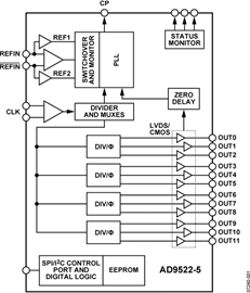
The AD9522 serial interface supports both SPI and I(2)C ports. An in-package EEPROM can be programmed through the serial interface and store user-defined register settings for power-up and chip reset.
The AD9522 features 12 LVDS outputs in four groups. Any of the 800 MHz LVDS outputs can be reconfigured as two 250 MHz CMOS outputs.
Each group of outputs has a divider that allows both the divide ratio (from 1 to 32) and the phase (coarse delay) to be set.
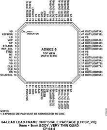
The AD9522 is available in a 64-lead LFCSP and can be operated from a single 3.3 V supply. The external VCO can have an operating voltage up to 5.5 V.
The AD9522 is specified for operation over the standard industrial range of -40°C to +85°C.
The AD9520-5 is an equivalent part to the AD9522-5 featuring LVPECL/CMOS drivers instead of LVDS/CMOS drivers.
(1)The AD9522 is used throughout this data sheet to refer to all the members of the AD9522 family. However, when AD9522-5 is used, it is referring to that specific member of the AD9522 family.
Applications
在集成度高度发展的今天,不能靠多个晶振源来解决问题,而且一旦晶振固定那么它的灵活性和可移植性必然受到很大影响,所以一些时钟分频芯片应运而生,今天我们将举一个很有代表性的AD9522时钟分频芯片的典型应用来达到一个抛砖引玉的作用一、AD9522简介 1.外部特性 A D 9 5 2 2是一个多路时钟输出和分配功能的芯片,本身支持亚皮秒抖动性能,在芯片内部还集成了PLL(PhaseLo
AD9520/AD9522时钟发生与分配IC,实现最佳器件集成度、低噪声、低抖动性能与信号输出灵活性全球领先的高性能信号处理解决方案供应商,最新推出一对时钟发生与分配IC——AD9520与AD9522,AD9520与AD9522多输出时钟发生器内置一个512Byte的嵌入式EEPROM存储器模块,为系统工程师提供了可用作时钟源和系统时钟的双重可编程时钟解决方案。通过利用片上存储
,最新推出一对时钟发生与分配IC——AD9520与AD9522,实现了业界最佳的器件集成度、低噪声、低抖动性能与信号输出灵活性的完美组合。AD9520与AD9522多输出时钟发生器内置一个512Byte的嵌入式EEPROM存储器模块,为系统工程师提供了可用作时钟源和系统时钟的双重可编程时钟解决方案。
【用 途】 场效应直流/调频/甚高频管 【性能 参数】N沟 27V 7-12mA 0.25W 100MHz 【互换 兼容】
双极型555定时器的电源电压范围为5~16 V,最大负载电流可达200 mA。CMOS555定时器电源电压范围为3~18 V,最大负载电流小于4 mA。所以,555定时
该荧光灯电子镇流器电路由电源电路、高频振荡器和LC串联输出电路组成。 电路中,电源电路由熔断器FU、电子滤波变压器T1、电容器C1、C2、压敏电阻器RV和整流二极管VD1 VD4组成;高频振荡器电路由晶体管V1、V2,二极管VD5、V D6、电阻器R1一R6、电容器C3一C5和高频变压器TZ组成;LC串联输出电路由限流电感器L、电容器C6、C7和荧光灯管EL组成。 接通电源,交流电压经T1和C1高
此前有消息称,小米新旗舰机小米5/5 Plus可能会于11月份发布。而通过外媒的最新消息,小米5/5 Plus将采用全金属机身,以及无边框设计。值得一提的是,小米5还可能会拥有两种不同内存版本,售价或为2300元。下面就详情来看看吧,希望会对大家有所帮助的据了解,小米5/5 Plus都将搭载骁龙820处理器。
【用 途】 差分放大器【性能 参数】 采用SO-8封装,采用3V、5V、±5V工作电源,并针对这些工作电源拟订技术规格,具5MHz截止频率和0.5dB纹波的四阶低通滤波器,82dBS/N(采用3V电源和2VP-P输出),低失真,2VP-P,800Ω负载,1MHz:93dBc(二阶),96dBc(三阶),全
【用 途】 低噪声运算放大器【性能 参数】 采用扁平 (1mm) ThinSOT 8脚封装。噪声为0.95nV/rtHz,工作在2.5V至12.6V的单电压或多个电压,静态电流小于1.8mA。增益带宽800MHz,斜率250V/us,增益稳定在10或更高。工作温度为-40℃至85℃。&nbs
【用 途】 反激开关电源控制电路【性能 参数】 采用6脚封装,输入电压可低至5V,输出电压精度±1.5%,静态电流仅为240μA,工作温度从-40℃到150℃,可用于12V和42V汽车电源。 是一款恒定频率、电流模式、反激式控制器,专为在高输入电压应用中驱动 N 沟道