0

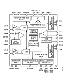
The dual ADC core features a multistage, differential pipelined architecture with integrated output error correction logic. Each ADC features wide bandwidth differential sample-and-hold input amplifiers supporting a variety of user-selectable input ranges. An integrated voltage reference eases design considerations. A duty cycle stabilizer is provided to compen-sate for variations in the ADC clock duty cycle, allowing the converters to maintain excellent performance.
The AD9640 has several functions that simplify the automatic gain control (AGC) function in the system receiver. The fast detect feature allows fast overrange detection by outputting four bits of input level information with very short latency.
In addition, the programmable threshold detector allows moni-toring of the incoming signal power using the four fast detect bits of the ADC with very low latency. If the input signal level exceeds the programmable threshold, the fine upper threshold indicator goes high. Because this threshold is set from the four MSBs, the user can quickly turn down the system gain to avoid an overrange condition.
The second AGC-related function is the signal monitor. This block allows the user to monitor the composite magnitude of the incoming signal, which aids in setting the gain to optimize the dynamic range of the overall system.
The ADC output data can be routed directly to the two external 14-bit output ports. These outputs can be set from 1.8 V to 3.3 V CMOS or 1.8 V LVDS.
Flexible power-down options allow significant power savings, when desired.
Programming for setup and control is accomplished using a 3-bit SPI-compatible serial interface.
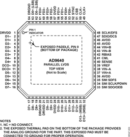
The AD9640 is available in a 64-lead LFCSP and is specified over the industrial temperature range of -40°C to +85°C.
Product Highlights
Applications
AD9640用于支持要求低成本、小尺寸和多功能的通信应用。 这款双ADC内核具有输出误差校正逻辑电路的多级差分管道体系结构。每颗ADC具有支持多种用户可选输入范围的宽带宽差分采样保持模拟输入放大器。
基于AD9640的无线接收机设计在无线接收机射频前端硬件的实际制作中,中频频率的选择、带通滤波器的中心频率与3dB带宽、外部无源器件的使用等设计考虑,都需要随着不同的系统应用而仔细的规划与调整,以便在适当的成本下达到规定的性能
美国模拟器件开发出了采样速度最高达150M样本/秒的14位A-D转换器“AD9640”。主要面向第3代移动电话和WiMAX等基站设备。
在无线接收机射频前端硬件的实际制作中,中频频率的选择、带通滤波器的中心频率与3dB带宽、外部无源器件的使用等设计考虑,都需要随着不同的系统应用而仔细的规划与调整,以便在适当的成本下达到规定的性能。本文以认知抗干扰为设计目标,主要讨论了接收机链路的核心器件之一高性能的ADC,叙述它们如何满足
美国模拟器件开发出了采样速度最高达150M样本/秒的14位A-D转换器“AD9640”。主要面向第3代移动电话和WiMAX等基站设备。