0

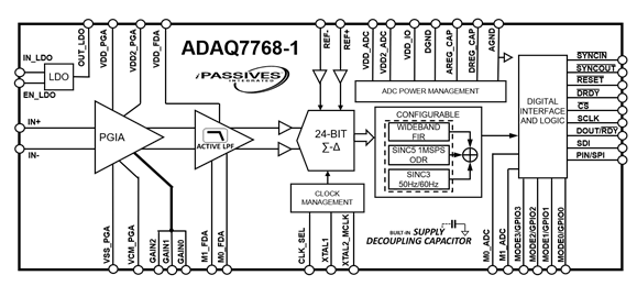
The ADAQ7768-1 is a 24-bit precision data acquisition (DAQ) μModule system that encapsulates signal conditioning, conversion and processing blocks into one system in package (SiP) design that enables rapid development of highly compact, high performance precision DAQ systems.
The ADAQ7768-1 consists of:
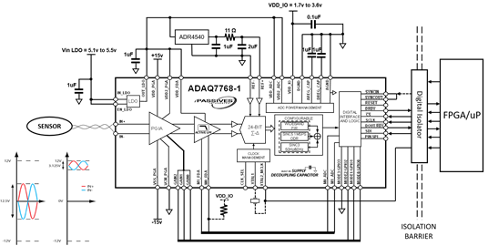
The ADAQ7768-1 supports fully differential input signal with a maximum range of ±12.6V. It has an input common mode voltage range of ±12V with excellent common mode rejection ratio (CMRR).
The input signal is fully buffered with very low input bias current of 2 pA typical. This allows easy input impedance matching and enables the ADAQ7768-1 to directly interface to sensors with high output impedance.
The seven pin-configurable gain settings offer additional system dynamic range and improved signal chain noise performance with input signals of lower amplitude.
A 4(th) order low-pass filter combined with the user programmable digital filter ensures the signal chain is fully protected against the high frequency noise and out of band tones presented at the input node from aliasing back into the band of interest. The low pass filter is carefully designed to achieve high phase linearity and maximum in-band magnitude response flatness. Constructed with Devices’s iPASSIVES technology, the resistor network used within the low-pass filter possess superior resistance matching in both absolute values and over temperature. As a result, the signal chain performance is maintained with minimum drift over temperature and the ADAQ7768-1 has an excellent device to device phase matching performance.
A high-performance ADC driver amplifier ensures the full settling of the ADC input at the maximum sampling rate. The driver circuit is designed to have minimum additive noise, error and distortion while maintaining stability. The fully differential architecture helps maximizing the signal chain dynamic range.
The to digital converter (ADC) inside the ADAQ7768-1 is a high performance, 24-bit precision, single channel Sigma-Delta converter with excellent AC performance and DC precision and the throughput rate of 256 kSPS from a 16.384 MHz MCLK.
An optional linearity boost buffer can further improve the signal chain linearity.
The ADAQ7768-1 is specified with the input reference voltage of 4.096V, but the device can support reference voltages ranging from VDD_ADC down to 1V.
The ADAQ7768-1 has two types of reference buffers. A pre-charge reference buffer to ease the reference input driving requirement or a full reference buffer to provide high impedance reference input. Both buffers are optional and can be turned off through register configuration. ADAQ7768-1 supports three clock input types: crystal, CMOS or LVDS.
Three types of digital low pass filters are available on the ADAQ7768-1. The wideband filter offers a filter profile similar to an ideal brick wall filter, making it a great fit for doing frequency analysis. The Sinc5 filter offers a low latency path with a smooth step response while maintaining a good level of aliasing rejection. It also supports an output data rate up to 1.024 MHz from a 16.384 MHz MCLK, making the Sinc5 filter ideal for low latency data capturing and time domain analysis. The Sinc3 filter supports a wide decimation ratio and can produce output data rate down to 50 SPS from a 16.384 MHz MCLK. This combined with the simultaneous 50/60Hz rejection post filter makes Sinc3 filter especially useful for precision DC measurement. All the three digital filters on the ADAQ7768-1 are FIR filters with linear phase response. The bandwidth of the filters, which directly corresponds to the bandwidth of the DAQ signal chain are fully programable through register configuration.
The ADAQ7768-1 also supports two device configuration methods. The user has the option to choose to configure the device via register write through its SPI interface, or through a simple hardware pin strapping method to configure the device to operate under a number of pre-defined modes.
A single SPI interface supports both the register access and the sample data readback functions. The ADAQ7768-1 always acts as a SPI slave. Multiple interface modes are supported with a minimum of three IO channels required to communicate with the device.
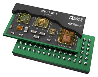
ADAQ7768-1 also features a suite of internal diagnostic functions that can detect a broad range of errors during operation to help improving the system reliability. The ADAQ7768-1 device has an operating temperature range of -40°C to +105°C and is available in a 12mm x 6mm, 84-ball BGA package with 0.8mm ball pitch. The ADAQ7768-1 utilizes only 75sq mm of board space, 10 times less than the discrete solution that utilizes 750sq mm.
Applications
1/2.5、1/1.8、1/1.6CCD尺寸图示对比,1/2.5、1/1.8、1/1.6CCD尺寸图示对比 1/2.5、1/1.8、1/1.6CCD尺寸图示对比经常看到关于CCD大小的争论,今天有空用AUTOCAD把常见的1/2.5、1/1.8、1/1.6CCD尺寸作图示对比,图中的三个正方形就是上面三个尺寸对应的CCD大小(注意:1/2.5、1/1.8、
1+1+1>3 有两个概念,“三网合一”与“三网融合”,区别开二者的涵义,也就明确了“融合”的真谛。
在“1+1”并机供电系统的运行中,如果其中的UPS-1的输入电源发生故障时,如上图所示,此时的UPS-2继续在市电电源提供的交流电源的支持下,经双总线输出开关中的MOB-2开关向用户的负载提供高质量的逆变器电源与此同时,位于UPS-1中的逆变器由于失去交流旁路同步跟踪信号源,它会在并机逻辑控制命令的调控下,从“双总线输出开关柜”的汇流上取得UPS-2的输出电源信号,并用这个电源信号来作为UP
AD7892BRZ-1是一款12位精度、串行输出的模数转换器(ADC)芯片。以下是该芯片的详细品类、参数和应用领域:
【用 途】 运算放大器 【性能 参数】 采用小型8引脚LFCSP和8引脚SOIC封装,采用±5V至±15V双电源供电,典型失调电压仅70?V,失调漂移不到1uV/°C,噪声仅为0.86uVp-p(0.1Hz至10Hz),额定温度范围为−25°C至+85°C工业温度范
【用 途】 高速放大电路【性能 参数】 采用8引脚SOIC封装和6引脚SOT封装,工作电压3V至10V,工作温度-40摄氏度至+125摄氏度,低宽带噪声:1nV/&raDIC;Hz,低1/f噪声:2.4nV
LT3478-1主要是由一个升压式DC/DC变换器为主,给LED提供可设定的恒流电流。 主要特点: 可实现PWM调光,调节范围3000:1;输入电压范围宽,从2.8~36V;内部有4.5A、60m
AD7657-1是一款16 位6 通道的模/数转换芯片,内部含有6 个独立的A/D 转换器,可同时进行A/D 转换,具有转换精度高、速度快、功耗低、输入模拟信号幅度大、信噪比高等优点,其突出特点是可通过多个AD7656-1 级联形成菊花链实现多个通道
LT3484-1芯片是一款相机闪光灯电容充电IC,内部集成了一个高压NPN电源开关,利用2.5~8V的电池电压可将闪光灯电容快速充电至320V,变换效率达80%,远高于传统闪光灯电容充电器。 性能特点: (1)快速充电:LT3484-1的充电时间为4.6
【用 途】 彩显微处理器【性能 参数】 采用40脚封装。【互换 兼容】 引脚符号功能电压(V)1HVADJ高压调整1.712BRT亮度控制1.47