华强商城 被动器件(电容/电阻/电感) BOM配单 原厂专区 PCB制板 积分兑换
0
首页>IC索引

ad9461

16-Bit, 130 MSPS A/D Converter

ad9461产品信息:

概览

优势和特点

  • 130 MSPS guaranteed sampling rate (AD9461-130)
  • 78.4 dBFS SNR with 10 MHz input
    (3.4 V p-p input, 130 MSPS)
  • 77.1 dBFS SNR / 85 dBc SFDR with 170 MHz
    input (3.4V p-p input, 130 MSPS)
  • 83 dBc SFDR with 225 MHz input
    (3.4V p-p input, 130 MSPS)
  • TBD dBFS 2-tone SFDR with 170 MHz and 170 MHz (130 MSPS)
  • 60 fsec rms jitter
  • Excellent linearity
    DNL = ±0.6 LSB typical
    INL = ±4.0 LSB typical
  • 2.0 V p-p to 4.0 V p-p differential full-scale input
  • Buffered inputs
  • LVDS outputs (ANSI-644 compatible) or CMOS outputs
  • Data format select (offset binary or twos complement)
  • Output clock available

产品详情

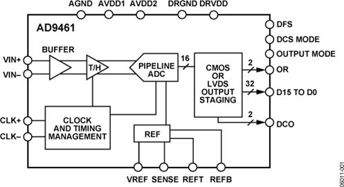
The AD9461 is a 16-bit, monolithic, sampling -to-digital converter (ADC) with an on-chip track-and-hold circuit. It is optimized for performance, small size, and ease of use. The product operates up to 130 MSPS, providing superior SNR for instrumentation, medical imaging, and radar receivers employing baseband (<100 MHz) and IF frequencies.

The ADC requires 3.3 V and 5.0 V power supplies and a low voltage differential input clock for full performance operation. No external reference or driver components are required for many applications. Data outputs are CMOS or LVDS compatible (ANSI-644 compatible) and include the means to reduce the overall current needed for short trace distances.

Optional features allow users to implement various selectable operating conditions, including input range, data format select, and output data mode.

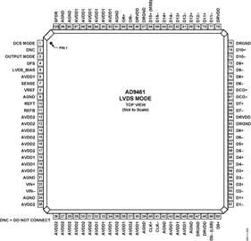
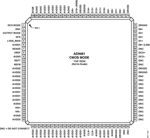
The AD9461 is available in a Pb-free, 100-lead, surface-mount, plastic package (100-lead TQFP/EP) specified over the industrial temperature range -40°C to +85°C.

Product Highlights

  1. True 16-bit linearity.
  2. High performance: outstanding SNR performance for baseband IFs in data acquisition, instrumentation, magnetic resonance imaging, and radar receivers.
  3. Ease of use: on-chip reference and high input impedance track-and-hold with adjustable input range and an output clock simplifies data capture.
  4. Packaged in a Pb-free, 100-lead TQFP/EP package.
  5. Clock duty cycle stabilizer (DCS) maintains overall ADC performance over a wide range of clock pulse widths.
  6. OR (out-of-range) outputs indicate when the signal is beyond the selected input range.


Applications

  • MRI receivers
  • Multicarrier, multimode cellular receivers
  • Antenna array positioning
  • Power amplifier linearization
  • Broadband wireless
  • Radar
  • Infrared imaging
  • Communications instrumentation


ad9461数据手册:

ad9461引脚功能、电路图:

AD9461

【用 途】 【性能 参数】【互换 兼容】

ADI推出差动放大器ADA4927

ADA4927可以使用单端/差动和差动/差动配置,并专为14位和16位转换器最佳化,包括ADI公司的AD9460和AD9461双信道16位ADC和AD9246低功耗14位ADC。

ADI两款16位ADC具79dB信噪比,速率达130MSPS

美国模拟器件公司(ADI)推出两款16位数据转换器AD9460和AD9461,并称具有业界最好信噪比(SNR)和中频(IF)取样性能,目标用在高端仪器仪表、医疗设备和无线通信应用,使设计者即使在高输入频率时也能保持有低噪音和高动态范围

相关型号:

AS ACT85610 ACT4921 ACT4911 ACT4910
ACT8945A ACT8892 ACT88760 ACT8870 ACT8865
ACT8849 ACT8847 ACT8846 ACT88430 ACT8840
ACT88329 ACT88327 ACT88326 ACT88325 ACT88321
按首字母检索