电子元器件产业互联网平台
电子元器件产业互联网平台


一站式电子元器件采购平台

元器件移动商城,随时随地采购

半导体行业观察第一站!

专注电子产业链,
坚持深度原创

电子元器件原材料采购
信息平台
摘要: [导读] Applications for clock data recovery (CDR) abound in telecommunications, optical transceivers, data and storage area networks, and wireless products. The benefits of CDR technology are increasingly important as designs require much greater
Applications for clock data recovery (CDR) abound in telecommunications, optical transceivers, data and storage area networks, and wireless products. The benefits of CDR technology are increasingly important as designs require much greater bandwidth, and as allocation and spectral bandwidth usage increase. Moreover, vendors and their products are migrating from parallel to serial interfaces for system- and board-level interfaces.
In recent years, the increased use of CDR technology has brimmed from the need to handle wider parallel bus widths across backplanes while managing clock and data skew at the receiver. Additionally, routing these signals can be difficult because they consume board space and power, and require multilayer routing schemes to manage signals and line termination. EMI generation from the use of high bit-width data buses is also a concern.
CDRs are extremely important due to the advent of new communication technologies, improvements in electrical signal processing, and the need to send multigigabit electrical signals across FR-4 and backplanes, optical, and wireless media. Communication techniques that combine clock and data prior to transmission are not new. The combination of clock and data ensure that the clock and data signals always arrive at the same time. The trick, however, is the separation of the clock and data at the receiver. This is accomplished by the CDR circuitry. Products that take data from a parallel to a serial format or vice versa are called serializers/deserializers (or "SerDes" for short). These products generally have CDR blocks to deserialize the serial data stream.
This article examines the component blocks of CDR needed to implement a successful CDR in high-speed serial-communication link applications. An overview of a typical high-speed serial-communication link is provided with respect to how data is transformed and recaptured over the link. Different CDR schemes are discussed with respect to the general CDR topology. Also, special attention is given to the reference oscillator's role on both the transmit and receive sides of the link.
Figure 1 provides a basic diagram of a high-speed serial-communications link. Parallel data (bits b1, b2, b3,... bn) arrives at the transmission serializer at frequency ft. Within the serializer, data is converted from the parallel format to a serial format. A serial-bit stream is developed with a minimum bit rate equal to n x ft, where n is the total number of parallel data bits. The resulting frequency (bit rate) can be higher than ft depending on whether the data is encoded to meet channel requirements for bit error rate (BER) performance or to provide rich transition content at the receive-side CDR. Reed-Solomon forward-error correction (FEC) and 8B10B encoding are, respectively, each examples of channel encoding or creating rich transition content at the receive CDR. This serial data is then readied for transmission to the channel and sent through to the receiver, finally reaching the deserializer. This basic communications block applies to data whether it is transmitted through fiber, air, or across backplanes.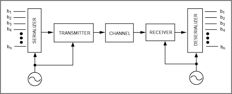
Figure 1. Clock and data recovery form the basis for high-speed serial communications links.
Timing (clocking) is critical in CDR applications. During system design, the designer determines how to drive data from a parallel format to a serial format for transmission and reception through the channel with pending channel distortion of the transmitted signal. Minimizing the effects of the design's degradation on the data signal is important for protecting signal-to-noise ratio and maintaining BER performance. For example, in digital-transmission schemes across backplanes, the system's jitter performance is extremely important as high-speed electrical signals traverse various lengths (FR-4 and the backplane), thus causing signal degradation in terms of signal-level and time-variant distortions.
At the core of clock-data recovery is a phase-locked loop (PLL)-based circuit that in some cases could be digitally based. Figure 2 is the basic PLL block diagram that could be used in the serializer or transmission side of the communication link shown in Figure 1. The PLL block includes a phase-frequency detector (PD), filter (LPF), voltage-controlled oscillator (VCO), and a divide chain (1/n). The divide chain is used to provide comparable frequency inputs to the PD. In this manner, the VCO's output is phase-aligned to the very stable reference input, VREF. This PLL block's purpose is to multiply the reference frequency by a fixed amount (n), which would be the VCO's natural frequency. In most cases, VREF would be quartz based, providing a high degree of stability and accuracy with great phase-noise characteristics. Additionally, this reference may be temperature compensated or voltage compensated, depending on the required application or system requirements. In SONET-based applications, this reference may meet a certain stratum level (i.e., stratum levels 3, 3E, or 4).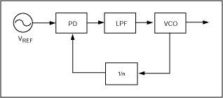
Figure 2. Clock multiplication applications are driven by PLLs.
At the receive side, the CDR PLL block takes on a slightly different look to address the need to retrieve both clock and data. As shown in Figure 3, the combined clock/data signal comes into the PLL block through a buffer that feeds two distinct paths. One path feeds the data-decision (DEC) block while the second path feeds the clock-recovery blocks. The clock-recovery blocks look very much like Figure 2's PLL block minus the 1/n block. The recovered clock from the VCO is used as a sampling input to the DEC, a feedback to the phase-frequency detector, and also to feed system-timing requirements downstream. In the case of Figure 1, this recovered clock is divided down to the parallel-clock frequency to drive the deserializer block.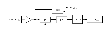
Figure 3. Modifications to the basic PLL block are used to implement CDR circuits.
The reference oscillators shown in the diagrams illustrate a VCO being applied to the input of the oscillator. This voltage control is established by the LPF stage. Typically, VCOs or voltage-controlled crystal oscillators (VCXOs) can be used as the loop oscillator, as shown in Figure 3. Primary to its role, the loop oscillator is required to track the frequency deviation of the incoming clock/data. Additionally, it provides this clock to other components downstream from the CDR (deserializer). This is accomplished by the output of LPF, which drives the voltage-control input of the VCO or VCXO.
In CDR applications for telecom, wireless, and datacom, the incoming data signal plus clock should have relatively stable frequency characteristics. This assumes the transmit clock meets certain accuracy and stability specifications. On the receive side, the design precludes for the minimum and maximum accuracy/stability. In the event the transmit clock frequency is expected to be with ±50ppm of a stated frequency, the receive clock would have frequency-adjustment capability of a minimum ±50ppm. For design purposes, however, consider a frequency adjustment capability somewhat larger than ±50ppm. This extended frequency-adjustment capability accommodates any additional signal-frequency distortion by the channel or disruptions in communications.
Although the PLL attempts to drive toward a static condition, meaning that frequency lock has been established, there could be conditions where the voltage-controlled input may move at higher rates than desired. The LPF bandwidth dictates the maximum rate at which the PLL can maintain lock. Ultimately, the role of the receive VCO (or VCXO) is to track and reproduce the recovered clock.
In the absence of a data/clock input into the CDR, the CDR is required for a specified time to provide a reference signal for any downstream communications requirements (i.e., the deserializer)
In some applications, a combination VCO/VCXO would be used. In Figure 4, VCO/VCXO allow for at least two benefits to the common CDR configuration. First, the addition of the VCXO allows fast regulation of the VCO frequency to match that of the expected clock/data signal. The VCXO frequency is chosen to match the expected clock frequency range. For example, a wideband VCO can require thousands of samples to lock onto the incoming data stream. The additions of the VCXO and lock-detection circuit ensure that the VCO maintains a certain operating frequency, and help provide a more predictable lock time in startup conditions. Second, the addition of the VCXO is helpful if the clock/data input has been lost over an extended period of time. In the absence of a clock/data signal, the system would refer to the very stable quartz-based oscillator (VREF) to provide holdover until the clock/data signal has been recovered from a loss of signal (LOS). Holdover is a specification that applies to the reference clock's ability to hold a certain accuracy over a certain period of time (for example, ±4.6ppm over 24 hours).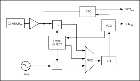
Figure 4. A modification on the basic CDR block provides easy locking on the incoming clock/data stream.
A variety of solutions address clock/data recovery and retiming, serializers and deserializers, clock generators, and TCXOs for communication applications. These devices allow designers to develop circuits for frequencies ranging from 10MHz up to 10GHz, and support applications ranging from GSM to OC-192 and above. As designs increasingly require greater bandwidth, CDR technology is ideal for telecommunications, optical transceivers, data and storage area networks, and wireless applications.

社群二维码

关注“华强商城“微信公众号
Copyright 2010-2023 hqbuy.com,Inc.All right reserved. 服务热线:400-830-6691 粤ICP备05106676号 经营许可证:粤B2-20210308