电子元器件产业互联网平台
电子元器件产业互联网平台


一站式电子元器件采购平台

元器件移动商城,随时随地采购

半导体行业观察第一站!

专注电子产业链,
坚持深度原创

电子元器件原材料采购
信息平台
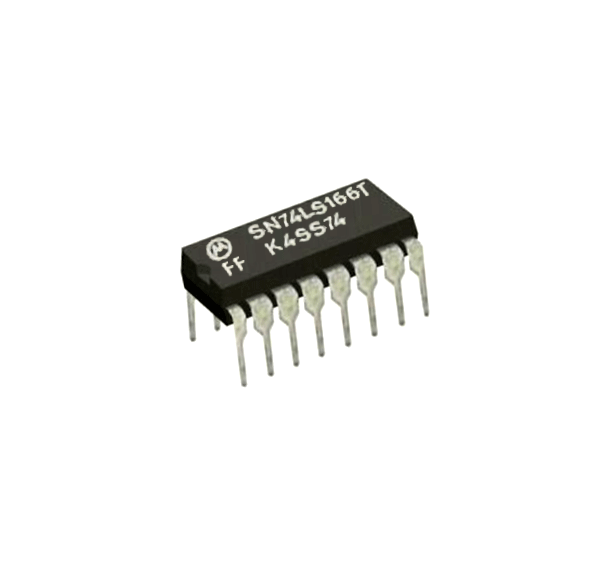
摘要: SN74LS166AN是与大多数其他TTL逻辑系列兼容的8位并行负载串行输出移位寄存器。该并行输入或串行输入,串行输出移位寄存器在单片芯片上具有77个等效门的复杂性。它具有门控时钟输入和优先清零输入。并行输入或串行输入模式由移位/负载输入建立。
SN74LS166AN是与大多数其他TTL逻辑系列兼容的8位并行负载串行输出移位寄存器。该并行输入或串行输入,串行输出移位寄存器在单片芯片上具有77个等效门的复杂性。它具有门控时钟输入和优先清零输入。并行输入或串行输入模式由移位/负载输入建立。
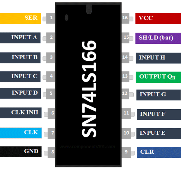
| Pin Number | Pin Name | Description |
| 2,3,4,5, 10,11,12,14 | A to H | Parallel Data inputs. Data on these inputs are asynchronously entered in parallel into the internal flip–flops when the Serial Shift/Parallel Load input is low |
| 13 | QH | Complementary Shift Register output Pin |
| 1 | SER | Serial Input Pin. When the Serial Shift/Parallel Load input is high, data on this pin is serially entered into the first stage of the shift register |
| 6,7 | CLK INH & CLK | Clock inputs. These two clock inputs function identically |
| 9 | CLR | Clear pin |
| 15 | SH/LD | Data–entry control input. |
| 18 | VSS | Ground |
| 16 | VCC | Supply Voltage – 5V, 10V, 15V |
8位 串行/并行至串行移位寄存器
工作电压:3V至18V
电源电压-最大:5.25 V
传播延迟时间:25 ns
最高 时钟频率:35MHz
工作温度范围:0C至+ 70 C
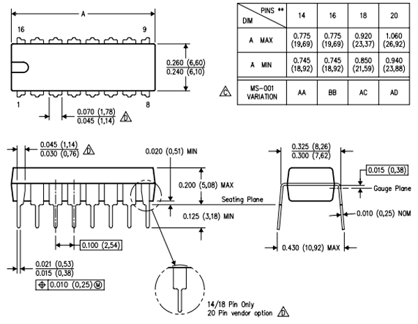
提供16引脚PDIP,GDIP,PDSO封装
| Name | Type |
| 74LS379 | Quad Parallel Shift Register |
| 4014 | 4 Bit static shift register |
| CD4035 | 8 Bit Shift Register |
| 74LS323 | 8 Bit Shift/Storage Register |
| 74LS164 | S/P Shift Register |
| 74HC595 | Dual 4 Bit Static Register |
| 74LS299 | 8 Bit Shift/Storage Register |
SN74LS166具有一个8位并行输入或串行输入,串行输出移位寄存器。意味着它可以串行或并行接收(输入)获取数据,并可以串行控制输出引脚。当我们的MCU / MPU上没有足够的GPIO引脚来控制所需数量的输出时,这非常方便。它通常用于必须通过微控制器控制相对大量LED的项目中。它也可以用作LCD屏幕的接口,因为它可以用作LCD显示器的数据位。
SN74LS166移位寄存器通常与微控制器或微处理器一起使用,以扩展GIPO功能。SN74LS166需要4线的微控制器。一种用于时钟,一种用于启用时钟,一种用于移位位,一种用于串行数据传输。要将 SN74LS166与微控制器一起使用,请将这四个引脚(SER,CLK INH和CLK和SH / LD )连接到微控制器的GPIO引脚。输入引脚(A到H)可以连接到某些类型的输入,例如按钮,开关等。
柜台,登记册
算术单位寄存器
左移-右移寄存器
串行到并行/并行到串行转换
序列产生
控制电路
代码转换

社群二维码

关注“华强商城“微信公众号
Copyright 2010-2023 hqbuy.com,Inc.All right reserved. 服务热线:400-830-6691 粤ICP备05106676号 经营许可证:粤B2-20210308